Замена полудохлого LPC2468
Пт июл 14, 2023 00:58:24
Привет всем!
Принесли в ремонт несколько промышленных плат с LPC2468.
Один совсем мертвый а на остальных помер один из входов где прицеплен датчик.
В общем нужно процессоры заменить, но тут у меня не хватает знаний.
По мануалу в проце 512 кб флешка.
Также по шине I2C прицеплена флешка 24С265
1. А может прошивка быть на этой флешке или только внутри проца или на SD карте?
2. Читать и писать эти процы через что и как?
UART0 на плате не разведен нормально. Но можно подпаяться.
3. Itag-а на плате нет. Но на колодку выведен I2C
4. Чтобы читать (ну пытаться) и писать проц нужно снимать с платы или будет достаточно подать 3.3 и Rx Tx
5. Какое ПО использовать? Нашел Flash Magic
6. А если проц залочен, что использовать для чтения (J-Link)?
Или в этом случае финиш и прочитать никак.
То есть мне не понятно, производитель может при производстве залочить от чтения, но оставить возможность обновления?
Помогите, просветите темного...
Re: Замена полудохлого LPC2468
Пт июл 14, 2023 01:06:31
https://www.nxp.com/docs/en/data-sheet/LPC2468.pdf писал(а):NXP Semiconductors designed the LPC2468 microcontroller around a 16-bit/32-bit
ARM7TDMI-S CPU core with real-time debug interfaces that include both JTAG and
embedded trace. The LPC2468 has 512 kB of on-chip high-speed flash memory.
DBGEN 9[1][8] F4[1][8] I DBGEN — JTAG interface control signal. Also used for boundary
scanning.
TDO 2[1][9] D3[1][9] O TDO — Test Data Out for JTAG interface.
TDI 4[1][8] C2[1][8] I TDI — Test Data In for JTAG interface.
TMS 6[1][8] E3[1][8] I TMS — Test Mode Select for JTAG interface.
TRST 8[1][8] D1[1][8] I TRST — Test Reset for JTAG interface.
TCK 10[1][9] E2[1][9] I TCK — Test Clock for JTAG interface. This clock must be slower than 1⁄6
of the CPU clock (CCLK) for the JTAG interface to operate.
RTCK 206[1][8] C3[1][8] I/O RTCK — JTAG interface control signal
7.2 On-chip flash programming memory.
The LPC2468 incorporates 512 kB flash memory system. This memory may be used for both code and data storage. Programming of the flash memory may be accomplished inseveral ways. It may be programmed In System via the serial port (UART0). The application program may also erase and/or program the flash while the application is running, allowing a great degree of flexibility for data storage field and firmware upgrades. The flash memory is 128 bits wide and includes pre-fetching and buffering techniques to allow it to operate at speeds of 72 MHz.
7.26.3 Code security (Code Read Protection - CRP)
This feature of the LPC2468 allows user to enable different levels of security in the system so that access to the on-chip flash and use of the JTAG and ISP can be restricted. When needed, CRP is invoked by programming a specific pattern into a dedicated flash location. IAP commands are not affected by the CRP. There are three levels of the Code Read Protection. CRP1 disables access to chip via the JTAG and allows partial flash update (excluding flash sector 0) using a limited set of the ISP commands. This mode is useful when CRP is required and flash field updates are needed but all sectors can not be erased. CRP2 disables access to chip via the JTAG and only allows full flash erase and update using a reduced set of the ISP commands.
Running an application with level CRP3 selected fully disables any access to chip via the JTAG pins and the ISP. This mode effectively disables ISP override using P2[10]/EINT0 pin, too. It is up to the user’s application to provide (if needed) flash update mechanism using IAP calls or call reinvoke ISP command to enable flash update via UART0.
Стоимость работы в случае 7.26.3 может легко стать шестизначной, притом не в самом начале диапазона...
Re: Замена полудохлого LPC2468
Пт июл 14, 2023 01:53:29
О, 6 значные значения...
Про Jtag был не прав был, есть разъем-площадки. Не признал, не заметил, виноват.
А чем пробовать читать?
Нашел ULINK mini в продаже...
Про Jtag был не прав был, есть разъем-площадки. Не признал, не заметил, виноват.
А чем пробовать читать?
Нашел ULINK mini в продаже...
Re: Замена полудохлого LPC2468
Вс июл 16, 2023 10:36:55
В общем проц не лоченый.
Купил J-Link проц прочитался.
Купил J-Link проц прочитался.
Re: Замена полудохлого LPC2468
Пн июл 17, 2023 11:40:44
1. А может прошивка быть на этой флешке или только внутри проца или на SD карте?
Только внутри.2. Читать и писать эти процы через что и как?
Flash Magic, JTAG.4. Чтобы читать (ну пытаться) и писать проц нужно снимать с платы или будет достаточно подать 3.3 и Rx Tx
Достаточно запитать, выставить нужный уровень BOOT-ног и снять RESET.6. А если проц залочен, что использовать для чтения (J-Link)?
Или в этом случае финиш и прочитать никак.
Финиш.Или в этом случае финиш и прочитать никак.
производитель может при производстве залочить от чтения, но оставить возможность обновления?
Может.Купил J-Link проц прочитался.
А что именно прочиталось? Файл состоящий из одних 0xFF? Re: Замена полудохлого LPC2468
Пн июл 17, 2023 12:11:51
Когда читал залоченный SM8958BW, оттуда читалось что-то отличное от 0xFF, но это была не программа. Так что не факт, что LPC прочитался.
Re: Замена полудохлого LPC2468
Пн июл 17, 2023 13:13:51
Прочиталась прошивка 
FF конечно есть но в конце.
Не по теме но все-же.
Я смотрел на поведение сбойных и рабочих плат.
К ним подключаются с десяток разъемов.
Но, стартуют и при нескольких (питания, 3 мотора, пара оптодатчиков) что сужает поиск сбойного места.
Сбойная проходит тест и ругаеться на один из оптодатчиков.
Прямо миганием светодиодов указывает какой.
Я проверил/разрисовал эту цепь. Сигнал через цифровые транзисторы и триггер шоттки попадает на цифровой вход проца.
Осциллограмма импульсов на этом входе на нормальной и на сбойной одинаковая (насколько я могу сравнить прямоугольные импульсы).
Из чего я сделал вывод что вход проца в порядке (хотя как я понимаю лучьше в разрыв поставить резистор и глянуть не его концах).
То что сбойная цепь того самого датчика на который указывает проц тоже вопрос хороший и не окончательный.
Никаких даташитов на плату конечно нет.
Если этот датчик откинуть - плата сразу в стоп падает.
Тут же вроде тест проходит но в конце ошибка.
Я считаю прошивку с рабочей платы.
Заменю горелый проц на новый и залью в него эту прошивку.
Потом попробую залить эту прошиву на сбойные - может это поможет.
Дальше сравню длительность и форму сигнала рабочей и сбойной - возможно тут косяк.
Ну а дальше, как я понимаю, смотреть в режиме отладки или пробовать диассемблировать прошивку чтобы понять на чем стопиться плата.
Добавлено after 2 minutes 3 seconds:
Ну я попробовал считать и зашить на одной из сбойных плат.
Работает.
FF конечно есть но в конце.
Не по теме но все-же.
Я смотрел на поведение сбойных и рабочих плат.
К ним подключаются с десяток разъемов.
Но, стартуют и при нескольких (питания, 3 мотора, пара оптодатчиков) что сужает поиск сбойного места.
Сбойная проходит тест и ругаеться на один из оптодатчиков.
Прямо миганием светодиодов указывает какой.
Я проверил/разрисовал эту цепь. Сигнал через цифровые транзисторы и триггер шоттки попадает на цифровой вход проца.
Осциллограмма импульсов на этом входе на нормальной и на сбойной одинаковая (насколько я могу сравнить прямоугольные импульсы).
Из чего я сделал вывод что вход проца в порядке (хотя как я понимаю лучьше в разрыв поставить резистор и глянуть не его концах).
То что сбойная цепь того самого датчика на который указывает проц тоже вопрос хороший и не окончательный.
Никаких даташитов на плату конечно нет.
Если этот датчик откинуть - плата сразу в стоп падает.
Тут же вроде тест проходит но в конце ошибка.
Я считаю прошивку с рабочей платы.
Заменю горелый проц на новый и залью в него эту прошивку.
Потом попробую залить эту прошиву на сбойные - может это поможет.
Дальше сравню длительность и форму сигнала рабочей и сбойной - возможно тут косяк.
Ну а дальше, как я понимаю, смотреть в режиме отладки или пробовать диассемблировать прошивку чтобы понять на чем стопиться плата.
Добавлено after 2 minutes 3 seconds:
Когда читал залоченный SM8958BW, оттуда читалось что-то отличное от 0xFF, но это была не программа. Так что не факт, что LPC прочитался.
Ну я попробовал считать и зашить на одной из сбойных плат.
Работает.
Re: Замена полудохлого LPC2468
Пн июл 17, 2023 13:17:08
вот если прокатит заливка на новые - тогда и можно сказать, что считалась прошивка. На сбойные может и прошивка не прокатить и не факт, что прошивка виновата, может, аппаратно что-то ушаталось.
Залочена может быть лишь часть прошивки
Проверять надо на новых.
Но мож и повезет... я как-то с ЭБУ автомобиля считал, дорогущего, тоже думал - наверняка залочена, а оказалось - заходи, бери что хочешь
Залочена может быть лишь часть прошивки
Проверять надо на новых.
Но мож и повезет... я как-то с ЭБУ автомобиля считал, дорогущего, тоже думал - наверняка залочена, а оказалось - заходи, бери что хочешь
Re: Замена полудохлого LPC2468
Пн июл 17, 2023 13:25:03
Потом попробую залить эту прошиву на сбойные - может это поможет.
Каким образом? Думаете прошивка восстановит сгоревшую ногу? (если уж нога сгорела)Насчёт проблемы в ноге МК - весьма сомнительно, раз сигнал проходит через много компонентов, а не напрямую с разъёма идёт. Искать проблему нужно в этих компонентах или в датчике, а не в прошивке МК.
Хотя конечно да: проще ведь искать не там где потеряли, а там где светлее.
Ну а дальше, как я понимаю, смотреть в режиме отладки или пробовать диассемблировать прошивку
Бессмысленная и бесперспективная затея. Тем более для человека, впервые их увидевшего.Ну я попробовал считать и зашить на одной из сбойных плат.Работает.
Т.е. - у вас что-то считалось (мусор?), потом - ничего не зашилось (в МК осталась исходная прошивка) и плата работает. Кто бы сомневался. Добавлено after 2 minutes 35 seconds:
Но мож и повезет... я как-то с ЭБУ автомобиля считал, дорогущего, тоже думал - наверняка залочена, а оказалось - заходи, бери что хочешь
Бывает, что в банке забудут закрыть сейф с золотыми слитками. Бывает. Может и повезёт. Re: Замена полудохлого LPC2468
Пн июл 17, 2023 13:57:54
Я считаю прошивку с рабочей платы.
Заменю горелый проц на новый и залью в него эту прошивку.
Потом попробую залить эту прошиву на сбойные - может это поможет.
Добавлено after 2 minutes 3 seconds:
Ну я попробовал считать и зашить на одной из сбойных плат.
Работает.
Заменю горелый проц на новый и залью в него эту прошивку.
Потом попробую залить эту прошиву на сбойные - может это поможет.
Добавлено after 2 minutes 3 seconds:
Ну я попробовал считать и зашить на одной из сбойных плат.
Работает.
за 2 минуты?!
Re: Замена полудохлого LPC2468
Пн июл 17, 2023 14:05:20
Кстати - здесь, на форуме есть соответствующий раздел для LPC2468. И называется он: "ARM".
Re: Замена полудохлого LPC2468
Пн июл 17, 2023 14:07:23
Конечно прошивка не восстановит горелую ногу.
Предварительно, уже были заменены все элементы, которые есть в цепи датчика.
Это не дало результата.
Также, я замерял падение напряжения на этой ноге и на других входах при снятом триггере.
Оно отличалось на обоих сбойных платах.
Поэтому возникло подозрение о проблеме именно этого входа.
Но, как оказалось, падение на рабочей плате аналогично сбойным.
В даташите процессора указано что у флешки есть ограничение на количество циклов записи. Аппарат не молодой.
Как написана прошивка я не знаю.
Возможно это проблема самой флешки или входа.
Вы пишите что может прочитаться мусор.
Так как понять что процессор не залочен?
Считать, затереть и проверить что чип пустой?
Re: Замена полудохлого LPC2468
Пн июл 17, 2023 14:09:55
если затереть, то и блокировка сотрется. будет просто новенький чип.
проверить можно либо заливкой на новый и проверкой всего функционала, либо тщательным изучением этого мк
проверить можно либо заливкой на новый и проверкой всего функционала, либо тщательным изучением этого мк
Re: Замена полудохлого LPC2468
Пн июл 17, 2023 14:24:13
Глянул дамп. Не мохоже что мусор.
Добавлено after 10 minutes 49 seconds:
По умолчанию J-Flash сначала затирает проц а потом шьет.
У меня так и было. Сначала стер, потом прошил.
Добавлено after 10 minutes 49 seconds:
Т.е. - у вас что-то считалось (мусор?), потом - ничего не зашилось (в МК осталась исходная прошивка) и плата работает. Кто бы сомневался. 
Добавлено after 2 minutes 35 seconds:

Добавлено after 2 minutes 35 seconds:
Но мож и повезет... я как-то с ЭБУ автомобиля считал, дорогущего, тоже думал - наверняка залочена, а оказалось - заходи, бери что хочешь
Бывает, что в банке забудут закрыть сейф с золотыми слитками. Бывает. Может и повезёт. По умолчанию J-Flash сначала затирает проц а потом шьет.
У меня так и было. Сначала стер, потом прошил.
Re: Замена полудохлого LPC2468
Пн июл 17, 2023 15:17:19
Глянул дамп. Не мохоже что мусор.
По дампу определили, без дизассемблера?? Вы видимо реально - гуру программирования.ЗЫ: Приблизительно можно глянуть по дампу начала прошивки - там должна быть таблица векторов прерываний, формат которой описан в мануале.
Можете просто сюда запостить дамп. Здесь есть знающие человеки.
По умолчанию J-Flash сначала затирает проц а потом шьет.
Это откуда такой вывод?Открываю свой проект-файл для LPC1758. Вижу:
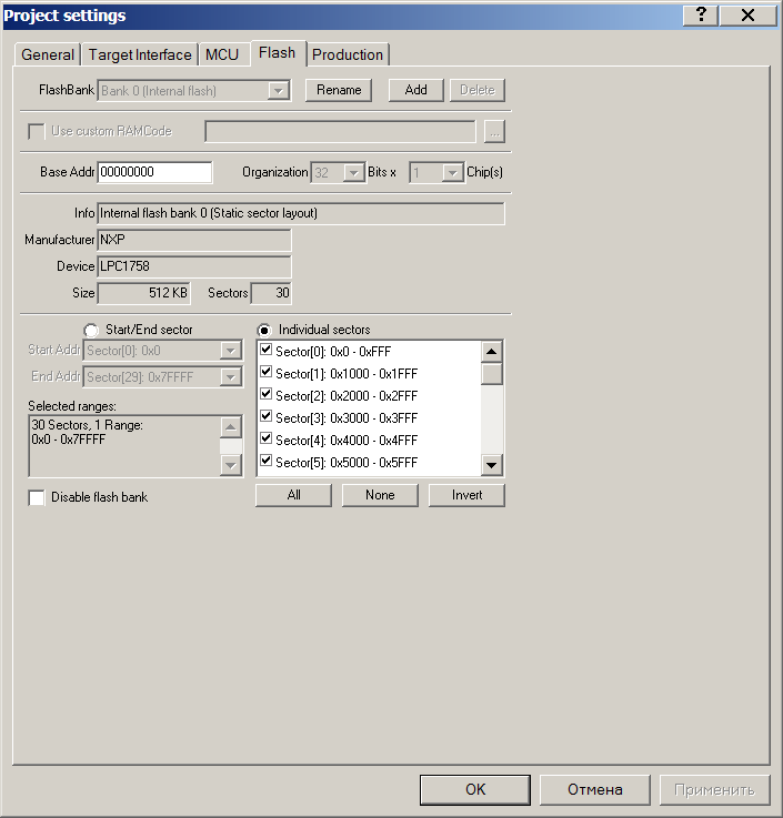
Видно, что в конфиг-файле определены номера секторов флешь стирания. JFlash может как стереть всю флешь, так и только сектора, занятые прошивкой (в зависимости от настроек). Стереть весь чип он может только по команде "Production programming" и то - если на вкладке ей соответствующей выбрано "стирать весь чип". По умолчанию там стоит посекторное стирание:
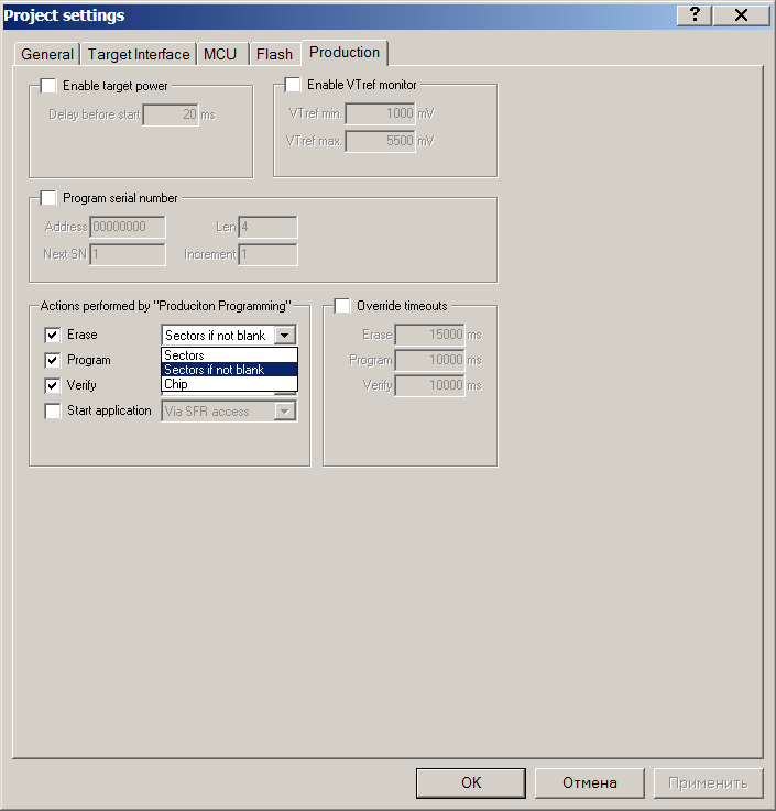
Да и "Production programming" - вы это делали?
Таким образом: Если в заливаемой вами новой прошивке (считанном дампе) указаны сектора, не относящиеся к началу флешь, то и исходная прошивка в МК окажется нестёртой. И выполняться будет она, а не то что вы думали что зашилось.
PS: LPC2468 похож по флешу на LPC1758.
Re: Замена полудохлого LPC2468
Пн июл 17, 2023 16:14:56
Я считывал флешку используя меню Read Back - Entire Chip
При это считывалось 28 секторов (504 Кб).
Настройки не менял, что J-Flash выставил то и использовал.
Потом делал Production Programming..
Внутри дампа есть текстовые строки поэтоу я предпологаю, что это не мусор.
Могу ошибаться и Entire Chip это не вся память, но тогда все мои телодвижения зря.
Новый процессор куплен, будет к концу недели. Вот и проверю что я начитал.
- Вложения
-
- Screenshot 2023-07-17 155730.jpg
- (93.51 KiB) Скачиваний: 25
-
- Screenshot 2023-07-17 155730.jpg
- (93.51 KiB) Скачиваний: 20
Re: Замена полудохлого LPC2468
Пн июл 17, 2023 18:36:36
Внутри дампа есть текстовые строки поэтоу я предпологаю, что это не мусор.
Текстовые строки - не надёжно. Если скажем - не прочитался первый сектор, то строки будут, но прошивка работать не будет. Ещё бывает - всякий мусор (типа строк) остаётся от предыдущих прошивок, когда отлаживаешь программу, так как каждая новая заливка затирает только необходимые ей сектора, и если раньше была большая прошивка, а заливается - меньшая, то за её хвостом останется мусор от старой. Хотя это вряд-ли ваш случай.Содержимое первого сектора - вектора прерываний - можно и визуально проверить их корректность (что я вам выше и предлагал).
Но дело ваше.
Re: Замена полудохлого LPC2468
Пн июл 17, 2023 21:21:09
Только добрался до компа.
Вот дамп.
Вот дамп.
- Вложения
-
- 2468 full 15.07.23.rar
- (78.73 KiB) Скачиваний: 27
Re: Замена полудохлого LPC2468
Вт июл 18, 2023 13:54:40
Вот дамп.
Выглядит нормальным. Похоже там реально в начале находится таблица векторов (8 элементов). 5-й элемент её (по адресу 0x14) должен содержать контрольную сумму остальных векторов (согласно документации на МК). Можете проверить. Остальные вектора у вас заполнены командой LDR PC, [PC, #24] (как и в моих прошивках), кроме 6-го вектора, указывающего на обработчик IRQ.
Re: Замена полудохлого LPC2468
Пт июл 21, 2023 09:45:35
Проц приехал.
Горелую плату восстановил, проц поставил, прошил и плата стартанула.
На днях подъеду поставлю на стенд а то без моторчиков и датчиков не проходит тест полностью.
Да, дамп с работающей платы аналогичен скачанному ранее.
Горелую плату восстановил, проц поставил, прошил и плата стартанула.
На днях подъеду поставлю на стенд а то без моторчиков и датчиков не проходит тест полностью.
Да, дамп с работающей платы аналогичен скачанному ранее.