Срыв работы импульсного PFM Step-Up преобразователя.
Пн мар 13, 2023 22:19:10
Была у меня мною сделанная схема отлично работала, пришлось изменить конструктив и переразвести плату и начался цирк и магия. Все компоненты одинаковые (переставлял с платы на плату) схема естественно не менялась, изменилась трассировка из визуального косяка вроде как теперь нет единых земляных полигонов, но это визуально, на самом деле плата 4 слоя и два внутренних слоя сплошная земля. Но в любом случаи шинками по верх я напаивал земли - не помогает. Один вариант платы работает и запускается стабильно всегда, второй только под нагрузкой и не стабильно...
Схема:
Вот собственно два варианта разводки:
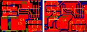
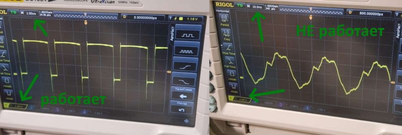
Как уже сказал детали все менял местами с платы на плату, разорванные полигоны шинками дублировал, вообще ничего не меняется, в первом варианте под любой нагрузкой все работает, есть стабильное управление, во втором CN3303 то и дело срывается в частоты за пределами рабочего диапазона визуально все работает да, но начинается просто жуткий перегрев транзистора и падает ток...
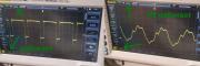
ОЧЕВИДНО что дело в разводке, но что именно...
Схема:
Вот собственно два варианта разводки:
Как уже сказал детали все менял местами с платы на плату, разорванные полигоны шинками дублировал, вообще ничего не меняется, в первом варианте под любой нагрузкой все работает, есть стабильное управление, во втором CN3303 то и дело срывается в частоты за пределами рабочего диапазона визуально все работает да, но начинается просто жуткий перегрев транзистора и падает ток...
ОЧЕВИДНО что дело в разводке, но что именно...
Re: Срыв работы импульсного PFM Step-Up преобразователя.
Пн мар 13, 2023 23:29:02
21 век, в чём проблема сделать чёткую картинку в png, как можно чтото понять в этом мыле. Всёравно 2 слой не видно.
В чём был смысл менять разводку, зачем вообще эта заливка, экономите хж ?
Если нет маски, могла и сопля прилипнуть.
Фото платы тоже не видно
В чём был смысл менять разводку, зачем вообще эта заливка, экономите хж ?
Если нет маски, могла и сопля прилипнуть.
Фото платы тоже не видно
Re: Срыв работы импульсного PFM Step-Up преобразователя.
Вт мар 14, 2023 00:15:13
21 век, в чём проблема сделать чёткую картинку в png, как можно чтото понять в этом мыле. Всёравно 2 слой не видно.
В чём был смысл менять разводку, зачем вообще эта заливка, экономите хж ?
Если нет маски, могла и сопля прилипнуть.
Фото платы тоже не видно
В чём был смысл менять разводку, зачем вообще эта заливка, экономите хж ?
Если нет маски, могла и сопля прилипнуть.
Фото платы тоже не видно
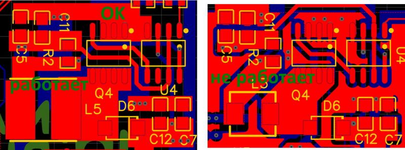
изменения все в верхнем (красном слое) обе разводки соответствуют схеме. Схема переразводилась под другой конструктив просто, ни элементы ни схема электрическая принципиальная не менялась. Немного грелась, количество меди и два внутренних слоя сплошной земли должны были убрать локальный нагрев... маска есть, соплей нет. Ради эксперимента с платы сдул все детали оставил только обвязку преобразователя, и один вариант двуслойной платы все отлично, а плата с земляными полигонами РАБОТАЕТ то же, выдает нужные напряжения, но управления идет явно не верное, частота подаваемого на затвор сигнала вне описанной в документации, ну и как следствие искажена форма и идет нагрев...
Вот она которая не работает, шинка на фото, это я подумал что земля между входными конденсаторами и транзистором плохая (через VIA идет)... но нет с такой доработкой она ведет себя ровно так же...

Re: Срыв работы импульсного PFM Step-Up преобразователя.
Вт мар 14, 2023 06:33:40
> изменения все в верхнем (красном слое)
Ага, я прям так и вижу что синий слой остался прежним.
Да, а раз он прежний - то зачем его кому-то смотреть... ))
Ага, я прям так и вижу что синий слой остался прежним.
Да, а раз он прежний - то зачем его кому-то смотреть... ))
Re: Срыв работы импульсного PFM Step-Up преобразователя.
Вт мар 14, 2023 09:21:05
В даташите обычно и разводку правильную рисуют и рекомендации. А что подать через потенциометр на fb и покрутить что будет там на входе на выходе?
Добавлено after 5 minutes 40 seconds:
В даташите заявлено что это зарядное, а не просто дсдс. Мб и не долдно без нагрузки запускаться? Мб в первый вариант просто повезло что работал преобразователь
Добавлено after 5 minutes 40 seconds:
В даташите заявлено что это зарядное, а не просто дсдс. Мб и не долдно без нагрузки запускаться? Мб в первый вариант просто повезло что работал преобразователь
Re: Срыв работы импульсного PFM Step-Up преобразователя.
Вт мар 14, 2023 09:52:02
Первым делом видно другое посадочное под дроссель. Он тот же самый? А ещё при перепайке могли компоненты помереть, особенно конденсаторы. Провода подводящие тоже имеют значение.
Re: Срыв работы импульсного PFM Step-Up преобразователя.
Вт мар 14, 2023 13:12:36
Первым делом видно другое посадочное под дроссель. Он тот же самый? А ещё при перепайке могли компоненты помереть, особенно конденсаторы. Провода подводящие тоже имеют значение.
посадочные разные, но я менял дроссели, ставил на рабочую плату с не рабочей и наоборот, от него ничего не зависело. Они аналоги по характеристикам просто разного производителя. Компоненты в одной закупке, но я сдувал все компоненты с плат вообще и ставил ВСЕ компоненты с рабочей платы на не рабочую, ситуация не исправлялась, компоненты одинаковые...В даташите обычно и разводку правильную рисуют и рекомендации. А что подать через потенциометр на fb и покрутить что будет там на входе на выходе?
Добавлено after 5 minutes 40 seconds:
В даташите заявлено что это зарядное, а не просто дсдс. Мб и не долдно без нагрузки запускаться? Мб в первый вариант просто повезло что работал преобразователь
Ну китайци редко делают хорошую документацию, у меня в руках был фабричный образец, ну и вобщем то первый вариант разводки (см ниже) прекрасно и очень стабильно работает (проповезло, это был не макет а мелкая серия, она все работает), я даже пытался его изуродовать, разрезов полигон между Q4 и С11 (как это в неудачной разводке происходит, там соединение через внутренний сплошной слой) - это не помешало работе... Что вы предлагаете подать и куда я не понял?Добавлено after 5 minutes 40 seconds:
В даташите заявлено что это зарядное, а не просто дсдс. Мб и не долдно без нагрузки запускаться? Мб в первый вариант просто повезло что работал преобразователь
> изменения все в верхнем (красном слое)
Ага, я прям так и вижу что синий слой остался прежним.
Да, а раз он прежний - то зачем его кому-то смотреть... ))
Ага, я прям так и вижу что синий слой остался прежним.
Да, а раз он прежний - то зачем его кому-то смотреть... ))
Исправляюсь!
Вот этот вариант работает, даже если снимать часть конденсаторов, резать полигоны (соединив их потом перемычкой тонкой в 1 см):

Это вот работает как описал выше, функционально верно, но в режим выходит только под нагрузкой большой, а с маленькой нагрузкой генерирует сигнал управления за пределами описанного в документации и как следствие завалы фронтов и нагрев:

Re: Срыв работы импульсного PFM Step-Up преобразователя.
Вт мар 14, 2023 13:49:57
> Ну китайци редко делают хорошую документацию
Получается что первый раз повезло, а во второй раз не очень.
PCB Considerations
A good PCB design is very important to efficiency and performance.
When laying out the printed circuit board, the following considerations should be taken to ensure proper operationof the IC.
If possible, use multi-layer PCB for better performance.
The ground connections of output capacitor, N-channel MOSFET, and catch diode (D2 in Figure 2)
need to feed into same copper that connects to the input capacitor ground before tying back into system ground.
This copper should be as wide as possible, and back to system ground separately.
To minimize radiation, the 2 diodes, MOSFETs, inductorand the input bypass capacitortraces should be kept as short as possible.
The connection between the diode and the MOSFETs should also be kept as short aspossible.
Place the inductor current sense resistor RCS right next to the input capacitor and inductor but oriented such that the IC’s CSN and VIN traces going to RCS are not long.
The 2traces need to be routed to getheras a single pair on the same layer at any given time with smallest trace spacing possible.
Получается что первый раз повезло, а во второй раз не очень.
Re: Срыв работы импульсного PFM Step-Up преобразователя.
Вт мар 14, 2023 14:05:59
Получается что первый раз повезло, а во второй раз не очень.
не очень понимаю о чем речь когда мы говорим о везении, все согласно документации, во втором варианте даже еще ближе к ней, единственное что к шунту не параллельно идут линии но они отдельные и короткие. Про плохую документаций это был ответ на вопрос, нет ли у производителя примера разводки - нет примера нет. Все остальные "косяки" возможные в разводке были проверены (например полигон между Q4 и С11, я восстановил толстой шинкой) и на работу они не влияют существенно в данном конкретном случаи (не изменили ситуацию, добавление шинки не убрало проблему, а разрезание полигона на рабочей плате не создало проблемы). Давай если есть некие конкретные соображения их обсудим, в данном случаи мне уже просто интересно стало, попробую развандалить одну плату на слои если выйдет... и собрать (склеить) без сплошного земляного полигона... потому что пока это единственное отличие которое проверить не удается... хотя по логике этот сплошной полигон должен только улучшать качество работы... но раз даже всемогущий интернет ничего не может придумать, то...
PS тут на другом ресурсе разные эксперименты проделать предлагали, правда практически все я их уже проделал сам прежде чем по форумам полезть, так ак они вобщем-то были очевидны... Вот: https://forum.easyelectronics.ru/viewto ... 10&t=47645
Re: Срыв работы импульсного PFM Step-Up преобразователя.
Вт мар 14, 2023 14:22:45
> все согласно документации
Ну как жеж "согласно документации" если нет:
> The ground connections of output capacitor, N-channel MOSFET, and catch diode (D2 in Figure 2)
> need to feed into same copper that connects to the input capacitor ground before tying back into system ground.
> This copper should be as wide as possible, and back to system ground separately.
Правило не выполняется, причем ближе к рекомендации, на мой взгляд, было в первом варианте.
> The 2traces need to be routed together as a single pair on the same layer
Правило не выполняется, есть переходные.
> попробую развандалить одну плату на слои если выйдет...
Попробуй простым путем - обсверлить переходные в районе C7-C12, можно изолировать этот кусок меди от внутренннего слоя внешними разрывами и бросить перемычку.
Это всё для реализации рекомендации
"Входной, выходной конденсаторы и исток транзистора обязаны иметь точечное соединение, т.е. располагаться рядом и быть соединены одним полигоном.
Безразрывным, коротким, в виде одного пятака ... и уж точно без via."
в виде ближе к первому варианту.
Re: Срыв работы импульсного PFM Step-Up преобразователя.
Вт мар 14, 2023 14:52:10
>
Ну как жеж "согласно документации" если нет:
Ну как жеж "согласно документации" если нет:
про D2 от схемы где он есть, про то что входные и выходные должны быть рядом... вот образец разводки которую я брал за основу:

Через переходные идут измерительные цепи, ну да ладно я их прокидывал и в первом слое, да и общей шиной накрывал все разорванные полигоны... ситуацию это не меняло... отизолировать выход от внутреннего слоя не пробовал, спасибо, сейчас попробую... Что в первом что во втором случаи выходы и входы по земле соеденены в другом слое шинами толстыми с россыпью переходных...
Но на самом деле я накрывал сверху толстой общей шиной земли транзистора и входных и выходных конденсаторов, до этого, первый же эксперимент это был, а в рабочей плате наоборот резал единый полигон от транзистора и соединял его сантиметровым проводочком... это как я уже говорил ситуацию не изменило... так что дело очевидно в разводке но не в этой ее части ((((
Обратите внимание на картинку выше, там земля входных выходных и транзистора общая, но есть переходные на полигон земли нижний, так вот , я в своей схеме толстой шинкой прокладывал именно вот так же... так что... не могу найти сверло тонкое что бы отсверлиться от второго слоя, но что-то мне подсказывает что это тут непричем ((((
Re: Срыв работы импульсного PFM Step-Up преобразователя.
Вт мар 14, 2023 16:42:15
Ну из других существенных изменений тут видно только 2/7 пин.
Кстати референс в виде demo board вот тут: http://www.consonance-elec.com/en/stati ... 102013.pdf .
Кстати референс в виде demo board вот тут: http://www.consonance-elec.com/en/stati ... 102013.pdf .
Re: Срыв работы импульсного PFM Step-Up преобразователя.
Ср мар 15, 2023 01:07:23
в общем что реально заработало, но пока без объяснения причин, просто тыкаясь всюду, в разрыв перед затвором транзистора поставил резистор пару сотен ом, до этого ставил 10 ничего не изменилось, с парой сотен сильно стало лучше, ну и по диагонали кинул шинку от минуса входных к минусам выходных конденсаторов.... ставбильность значительно выросла, но все еще не идеально...
Re: Срыв работы импульсного PFM Step-Up преобразователя.
Ср мар 15, 2023 04:48:42
> с парой сотен сильно стало лучше
Ну по сути правильно, фронт затянулся, на паразитных индуктивностях меньше выброс
> ну и по диагонали кинул шинку от минуса входных к минусам выходных конденсаторов
С отрезанием от нижних слоев или без?
Ну по сути правильно, фронт затянулся, на паразитных индуктивностях меньше выброс
> ну и по диагонали кинул шинку от минуса входных к минусам выходных конденсаторов
С отрезанием от нижних слоев или без?
Re: Срыв работы импульсного PFM Step-Up преобразователя.
Ср мар 15, 2023 11:19:35
> с парой сотен сильно стало лучше
Ну по сути правильно, фронт затянулся, на паразитных индуктивностях меньше выброс
> ну и по диагонали кинул шинку от минуса входных к минусам выходных конденсаторов
С отрезанием от нижних слоев или без?
высверлил переходы, кинул, стало лучше, потом кинул на плате без высверливания, стало еще лучше, короче пока так... А про выбросы, я бы понял если бы контроллер возбуждался и не работал, он собака в возбуждении функционал то сохраняет, если бы не дикий нагрев транзистора, я бы и не заметил что есть проблема... но с затянутыми фронтами все же лишний нагрев будет и кпд подупадет.... так что плохо (Ну по сути правильно, фронт затянулся, на паразитных индуктивностях меньше выброс
> ну и по диагонали кинул шинку от минуса входных к минусам выходных конденсаторов
С отрезанием от нижних слоев или без?
ну и самое главное что все равно при низкой нагрузке те же проблемы... срыв на высокие частоты и все такое (
Re: Срыв работы импульсного PFM Step-Up преобразователя.
Ср мар 15, 2023 21:24:26
попробуй шунтирующую керамику 0,1 с 7 ноги на землю. питание микрухи бродит по всем злачным местам модуля, и приносит ей все помехи что там вообще есть.
Re: Срыв работы импульсного PFM Step-Up преобразователя.
Пт мар 17, 2023 15:29:16
попробуй шунтирующую керамику 0,1 с 7 ноги на землю. питание микрухи бродит по всем злачным местам модуля, и приносит ей все помехи что там вообще есть.
полагаю вы ближе всего оказались к разгадке, и ваш способ даже работает, не идеально, при низкой нагрузке после среза управляющего импульса на транзистор все равно есть небольшое возбуждение и звон, но все довольно стабильно и без нагрева.
Долго смотрел на образцово-показательные примеры разводки, в контексте моей рабочей и не рабочей, и вот что тут видно, на одной входные конденсаторы непосредственно связаны с землей CN3303, во-втором случаи земля вовсе отвязана от силовой части. У меня в примере который работает земля то же была довольно хорошо связана с входными конденсаторами это единственное визуальное отличие... ну что же, подумал я, отвяжемся от силовой земли, поднял я ногу 4 на CN3303 и коротким проводом кинул ее на конденсаторы входа, все, генерация, звон, да вообще все проблемы ушли тут же...

ВСЕМ СПАСИБО!
Re: Срыв работы импульсного PFM Step-Up преобразователя.
Пт мар 17, 2023 16:37:57
Так это и есть вот эта рекомендация:
The ground connections of output capacitor, N-channel MOSFET, and catch diode (D2 in Figure 2)
need to feed into same copper that connects to the input capacitor ground before tying back into system ground.
This copper should be as wide as possible, and back to system ground separately.
---
Ну, результат достигнут, это хорошо.
Будет новый вариант платы - показывайте )
Re: Срыв работы импульсного PFM Step-Up преобразователя.
Ср янв 10, 2024 11:54:52
zwitch, Здравствуйте! Приобрел данную плату готовую на Али. Это Ваша разработка?
Она отключает заряд при 8В +-0,1В. Следовательно дело не доходит до балансировки и по итогу недозаряжает банки. С этим что то можно сделать? Или выбросить и забыть?
Она отключает заряд при 8В +-0,1В. Следовательно дело не доходит до балансировки и по итогу недозаряжает банки. С этим что то можно сделать? Или выбросить и забыть?
Re: Срыв работы импульсного PFM Step-Up преобразователя.
Ср янв 10, 2024 14:02:45
zwitch, Здравствуйте! Приобрел данную плату готовую на Али...
нет, у меня плата на таком же чипе, это единственное общее место. И тут чип обсуждается который рассчитан на 3 ячейки, а не 2 (у вас похоже другая модель)
Последний раз редактировалось zwitch Ср янв 10, 2024 17:48:36, всего редактировалось 1 раз.